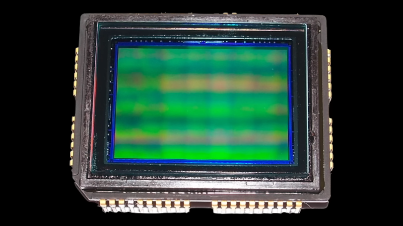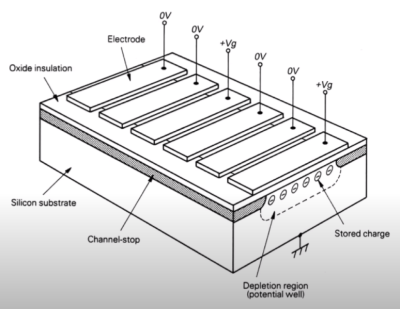

Have you ever thought how amazing it is that every bit of DRAM in your computer requires a teeny tiny capacitor? A 16 GB DRAM has 128 billion little capacitors, one for each bit. However, that’s not the only densely-packed IC you probably use daily. The other one is the image sensor in your camera, which is probably in your phone. The ICs have a tremendous number of tiny silicon photosensors, and [Asianometry] explains how they work in the video you can see below.
The story starts way back in the 1800s when Hertz noticed that light could knock electrons out of their normal orbits. He couldn’t explain exactly what was happening, especially since the light intensity didn’t correlate to the energy of the electrons, only the number of them. It took Einstein to figure out what was going on, and early devices that used the principle were photomultiplier tubes, which are extremely sensitive. However, they were bulky, and an array of even dozens of them would be gigantic.

CCDs opened up the digital image market, but it has some problems. The next stage was CMOS chips. They’d been around for a while since IBM produced the scanistor, but the sensitivity of these CMOS image chips was poor. Since most people were happy with CCD, there wasn’t as much research on CMOS. However, CMOS sensors would eventually become more capable, and the video explains how it works.
We’ve looked at image sensors before, too. The way you read them can make a big difference in your images.

